Project Goal: Restore a partially functioning PDP-8/L computer to a fully functional state.
Time Frame: 8 weeks.
History and Description of PDP-8/L
The PDP-8 family of computers were historically the first line of commercially successful general purpose computers. Designed by Digital Equipment Corporation (DEC) in the 1960s, they were the first computers to be sold on a retail basis in a table-top configuration. At the time of this writing, functional units still exist, serving as vintage collectibles and as academic teaching tools for computer architecture.
The PDP-8/L utilizes Transistor-Transistor Logic Medium Scale Integration (TTL MSI) in a fully parallel implementation. Word size is 12-bits, divided into four sets of 3 bits represented in octal format. In a cost-saving design, the usage of registers was substantially reduced and substituted by memory. Only four 12-bit registers are present: the Accumulator, Program Counter, Memory-Buffer register, and Memory-Address register.
Components
Core Stack (Magnetic Core Memory)
The core stack consists of a 64 by 64 by 12 matrix of small toroidal ferrite-cores, which can hold a magnetic state to store a bit. Each core is threaded through by 4 wires: X-Selection, Y-Selection, Sense, and Inhibit.
Memory Select: Only the combined current of X-Selection and Y-Selection through a magnetic core will cause it to change state.
Read: Current is run through the X-Selection and Y-Selection wires in the direction that causes the selected magnetic cores to change to the ‘0’ state. During this destructive read, the magnetic cores that change state induce a current in the Sense wires, indicating a previously stored 1. Every Read is followed by a Write to restore the contents.
Write: A destructive read first changes the selected magnetic cores to the ‘0’ state. Afterwards, current is run through the X-Selection and Y-Selection wires in the direction that causes the selected magnetic cores to change to the ‘1’ state. To write a ‘0’, current runs through the Inhibit wire in the opposite direction of the Memory Select wires.
Documentation: Page 4-12 of “DEC PDP-8L Maintenance Manual Volume 1”.
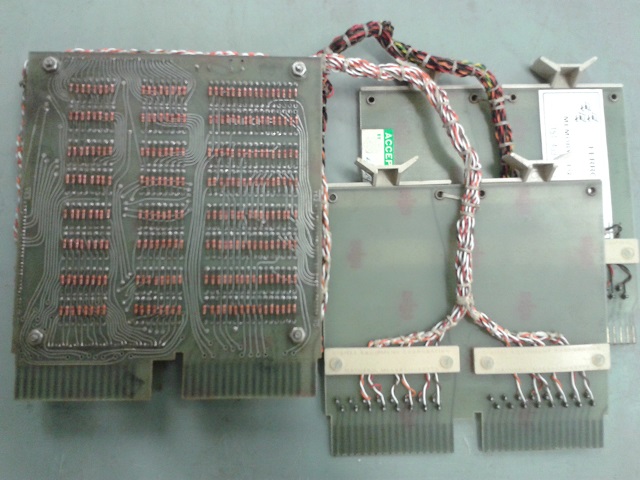
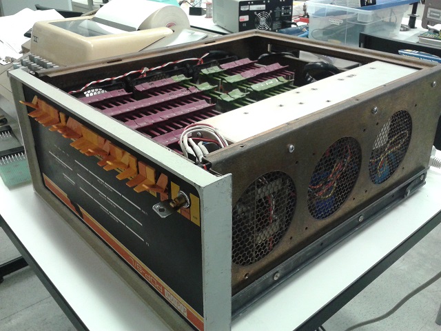
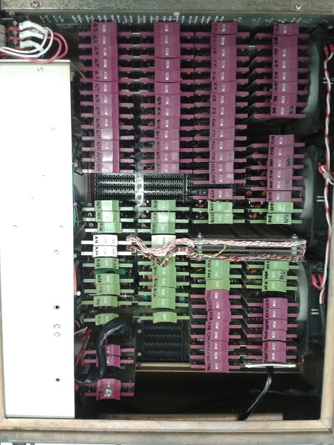
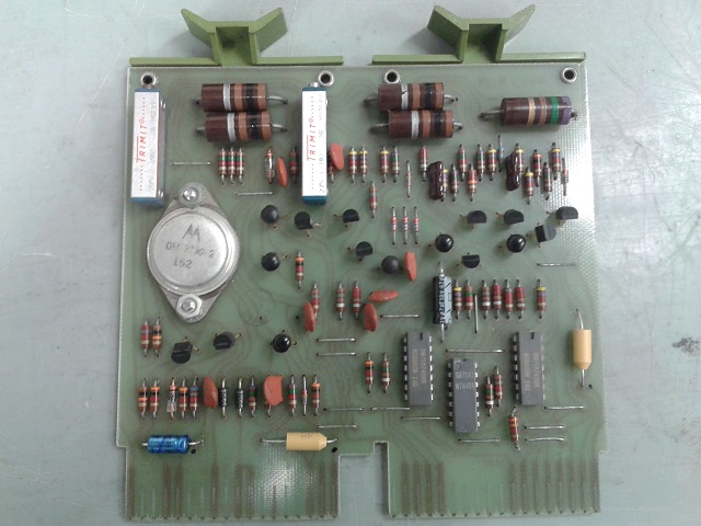
Flip Chip Modules
The circuit boards and logic components are divided into “Flip Chip” modules. The basic dimensions are 2 and 7/16 inches wide by 5 inches long, with an additional 1/2 inch handle. Each board contains 18-contact card edge connectors.
M220 Major Registers
Consisting of a pair of flip-chips, each M220 module is responsible for 2 bits of the major register bus, which drives the Accumulator.
- AB07: Bits 0, 1.
- AB06: Bits 2, 3.
- AB05: Bits 4, 5.
- AB04: Bits 6, 7.
- AB03: Bits 8, 9.
- AB02: Bits 10, 11.

G221 Memory Selector
The G221 Memory Selector decodes Memory Addresses to drive the X-Selection and Y-Selection wires in the core stack. Each pair decodes 3 out of the 12 bits in the address.
- C23 C24: Bits 0 – 2.
- D18 D19: Bits 3 – 5.
- C18 C19: Bits 6 – 8.
- D23 D24: Bits 9 – 11.
Within the pairs, one module will decode for the addresses 0 – 3 octal (000 – 011 binary), while the other will decode for the addresses 4 – 7 octal (100 – 111 binary).
- C19, C24, D18, D23: Addresses 0 – 3 octal, 000 – 011 binary.
- C18, C19, D19, D24: Addresses 4 – 7 octal, 100 – 111 binary.
Example: Memory Address 1573 will be decoded by C24, D19, C18, D23 respectively.

G020 Sense Amplifier
The G020 Sense Amplifier is responsible for amplifying the signal (if any) detected by the core stack Sense wires in order to detect a logical 1.
Each module is responsible for amplifying 2 bits out of the 12-bit word that is read from the core stack.
- A18: Bits 0, 1.
- A19: Bits 2, 3.
- A20: Bits 4, 5.
- B18: Bits 6, 7.
- B19: Bits 8, 9.
- B20: Bits 10, 11.

G228 Inhibit Driver
The G228 Inhibit Driver is responsible for driving the Inhibit wires during a write operation in the core stack.
Each module drives 4 out of the 12 bits.
- A23: Bits 0 – 3.
- B23: Bits 4 – 7.
- B24: Bits 8 – 11.

Restoration Log
Notes
Memory addresses are 12-bit and will be denoted in octal format. Example: 001 010 011 100 is address 1234.
Memory patterns will be shorthanded by the symbol ‘x’. Example: xx0x are memory addresses which contain octal 0 in the 3rd position.
Week 1
There had been several previous teams working on restoration of the PDP-8/L. The power supply, ventilation fans, and front panel had been previously restored. The computer can be safely powered on with system stability. Previously known good address is 5555. A document “Toggle-in Programs” to test the basic functions of the PDP-8/L is available.
First diagnostic is to determine the functional status of the core stack. Memory locations 0000 – 0007 were manually tested. A bit pattern of alternating 1s and 0s were written into memory and then subsequently read. Upon read, the memory buffer displays all 0s instead of the written bit pattern. Memory locations 5555 – 5557 were manually checked by writing a bit pattern of all 1s. Upon read, the memory buffer display correctly corresponds with the written bit pattern.
“Increment AC” from “Toggle-in Programs” was loaded at starting memory address 5555. However, the program did not execute as expected, as it was written for a different starting address 0200. Unfortunately, manual testing of the address at 0200 found that it was not functioning.
Preliminary study of the “Introduction to Programming” DEC PDP-8/L handbook provided enough information on the machine instruction format to rewrite “Increment AC” with starting address 5555. The program executed as expected, demonstrating that the IAC, ISZ, and JMP instructions, as well as the Accumulator register were functional. Successful toggling-in of the program also implies that the Program Counter, Memory Address, and Memory Buffer registers were functional.

Week 2
Further study of the “Introduction to Programming” DEC PDP-8/L handbook from last week provided complete information of the PDP-8/L machine instructions and addressing format, as well as the front panel switches. This information was personally summarized in the pdf document “PDP-8 Computer and ASR-33 Teletype Programming Info”.
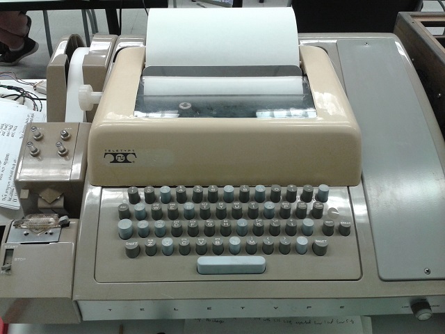
The PDP-8/L was designed to interface with the ASR-33 Teletype. There was one unit (Unit A) available in the lab that is functional but with faded print quality. The ink ribbon was changed numerous times with new ink ribbons, but no improvement was seen. The hard rubber on the print head had become brittle; it was scraped off and replaced with hard plastic. Unfortunately, there was still no improvement in print quality. Nonetheless, the unit was fully functioning, with each key printing the correct character.
The W076 flip-chip module “Teletype Connector” is required to interface the PDP-8/L with the teletype. The spare W076 available in the lab had been connected to a standard DE-9 connector. However, Unit A had been modified with a non-standard external connector by its previous owner. The connector was removed, and the wires traced back into the teletype for rewiring with a standard DE-9 connector. Comparisons were made with a separate teletype (Unit B) which had a standard DE-9 connector in order to facilitate the rewiring. Documentation of the W076 standard connection with the teletype was found after the rewiring, which fortunately confirmed that the rewiring was correct.
The rewired teletype was connected to the PDP-8/L, and a basic “Print Test” program from “Toggle-in Programs” was executed to test output. The program executed as expected, with the teletype printing every ASCII character. Next, “Echo Test” from “Toggle-in Programs” was executed to test input. The program also executed as expected, with each key-press on the teletype registering correctly in the Accumulator, before being retransmitted to the teletype for printing.
Due to the unsatisfactory print quality of the teletype, a different unit (Unit C) was sought out and rewired with a standard DE-9 connector. However, Unit C did not function as expected, and was theorized to be constantly running in Line mode. Comparisons were made with (Unit A), and a wire connection was found to have been cut and spliced to a jumper, possibly to facilitate remote control. This wire connection was restored and Unit C functioned as expected. Unit C was connected to the PDP-8/L and both “Print Test” as well as “Echo Test” were successfully executed. The print quality of Unit C was better than Unit A, thus Unit C was chosen to be the teletype for the workstation.


Week 3
With a working teletype unit, a program “Memory Check” was written to check each memory location and print if there is an error. The program works by first writing a bit pattern into an address location and immediately reading from that address location. If the read value is different from the written value, the program would print the address to the teletype in human-readable format, before moving on to the next address.
Memory locations 5410 – 5527 were manually hand-checked with bit pattern 0000 and 7777 in order to find sufficient contiguous memory for “Memory Check”. Fortunately, there is just enough space to load in this program. The purpose of this program is to print out memory addresses with errors to see if any patterns emerge. It is also an indirect test of the various machine instructions which were utilized. After some debugging, the program executed successfully. There are some minor spacing errors in the print with some lines slightly overlapping, as there is insufficient delay between “Carriage Return”, “Line Feed”, and the next character to print. This problem could be solved by modifying the program to have two “Line Feed”, but memory space constraints prevented this solution.
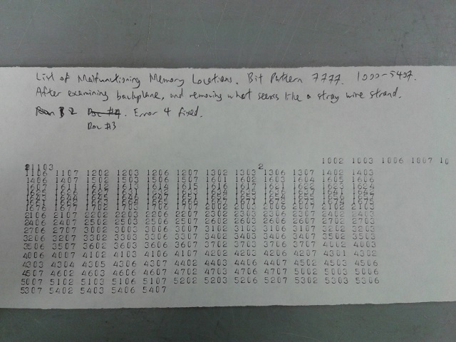
In the 1st run of the “Memory Check” program, four patterns in the memory errors can be observed: 0xxx (Error 1), xx0x (Error 2), 16xx (Error 3), and 43xx (Error 4). The core stack was found to be mostly working. The error patterns imply that only the components responsible for those memory bit positions were malfunctioning.
A possible troubleshooting method is to swap the flip-chips within the PDP-8/L responsible for certain bits of memory, in order to see if the error pattern changes predictably. Each flip-chip within the PDP-8/L had previously been marked with its original location, possibly by the previous teams. The G221 flip-chips at C23 C24 were swapped with those at D23 D24 and “Memory Check” executed. However, Error 1 did not predictably change to 000x, and there was no other noticeable change in the error pattern.


Week 4
The backplane of wire-wrap was checked for possible short circuits or damaged wiring. Repairs had been done by the previous team. There was a loose strand at the end of a repaired wire that was suspected of causing a short circuit. It was removed along with other bits of dust and strands of hair. “Memory Check” was executed again, and Error 4 (43xx) seems to have been resolved.
Two spare G221 flip-chips were refurbished by replacing and re-soldering the ICs and electrolytic capacitors. They were swapped into the PDP-8/L to determine if any of the original G221 flip-chips were faulty. This resulted in the contents of the addressed memory to be erased, in the affected locations which are decoded by the refurbished G221s. By swapping in the refurbished G221s one at a time, It was determined that one of them was faulty, while the other did not produce any different results.
The functioning refurbished G221 was swapped into C19 and “Memory Check” executed. Error 2 (xx0x) did not predictably change location as expected. The refurbished G221 was swapped into D19, yet “Memory Check” showed no change in error pattern. The refurbished G221 was removed, and the originals placed back in. The G221s at C23 C24 was swapped with D23 D24, but Error 1 (0xxx) still remains at the same location.
As the faulty refurbished G221 consistently erased memory at address locations which it was responsible for decoding, it was used to determine the responsible address locations of each G221 location, which was cross-checked with documentation (DEC PDP-8/L Schematics, D-BS-8L-0-15/16). This exercise and the results of the previous “Memory Check” runs implied that the original G221s were most probably functional.
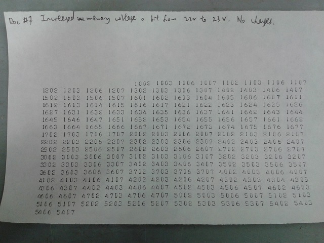
By inspection of the G785 “Power Connector”, the voltage supplied to memory was slightly lower than the recommended value. Based on the Memory Alignment Procedure on page 5-7 of “DEC PDP-8L Maintenance Manual Volume 1”, the trimpot on the G826 “Regulator Control” was adjusted to increase the Memory Supply Voltage. “Memory Check” was executed again, but there was no change in error patterns.
There is a spare core stack which was swapped in with a few memory locations manually hand-checked. Its performance was different than the original core stack, which implied the possibility that the original core stack itself might have malfunctioning components. The diodes on the original core stack were examined with a multimeter, and a total of 10 diodes were found to be faulty. The positions of these diodes were noted down for further troubleshooting.


Week 5
During removal of the faulty diodes, a trace was accidentally damaged. Fortunately, schematics were available of the interconnections between the diodes, and the electrical connection can be repaired. Equivalent replacement diodes for the core stack were not immediately available in the lab. Instead, the diodes on the spare core stack were de-soldered and used. This would guarantee that the replacement diodes are equivalent. As the solder pads were hard to reach by hand, and to prevent damaging the traces underneath, a different soldering technique was used. Resistor leads were first soldered onto the board, then the diode leads were wrapped around the resistor leads and soldered in place, before cutting off the resistors.
“Memory Check” was executed to test the core stack, and no errors were reported. To double-confirm, “Memory Check” was altered to print if the memory location is OK. The teletype proceeded to print every memory location, signifying that the core stack is now fully functional. Unfortunately, the “Line Feed” of the teletype stopped working halfway through the printing.
Paper tapes of the BIN loader and other programs were available, while the RIM loader is short enough to be toggled-in by hand. The low-speed paper tape reader of the teletype works; the BIN loader was successfully loaded and used to load a non-original paper tape copy of a DEC diagnostic program “Memory Checkerboard (Low)”.

According to documentation of “Memory Checkerboard”, the program tests memory for core failure under worst case conditions. The Low version occupies memory locations 0005 through 0105 and tests memory from 0151 through 7700. The High version occupies memory locations 7430 through 7573, and tests memory from 0000 through 7400. The programs will not automatically halt unless an error in memory is encountered. If they halt, they will display in the Accumulator the erroneous memory address and its contents.
“Memory Checkerboard (Low)” halts at each memory address even though the Accumulator shows no error in the memory contents. The original paper tape of the “Memory Checkerboard (Low)” was loaded, and this problem was no longer encountered, implying that the paper tape copy is not perfect. The original “Memory Checkerboard (Low)” only halts intermittently at memory locations 16xx, with 1 or 2 bits of the contents being erroneous. Manual checking of memory locations 16xx by hand show no errors, which implies that those memory locations are mostly functional except under worst-case conditions. Curiously, “Memory Checkerboard (High)” does not halt, which implies that all memory locations are functional.
Backup copies of the original “Memory Checkerboard (Low)” and “Memory Checkerboard (High)” paper tape were made with the teletype paper punch. The documentation ID for “Memory Checkerboard” is “MAINDEC-08-D1L0”.
Various original DEC paper tape programs and copies.
Week 6
In an attempt to fix the “Line Feed” problem on the teletype, its internal mechanical components were observed while running. The observations were compared to another spare teletype unit, and it was found that a small plastic separator piece was missing, which had most probably gotten loose and fallen off. A small piece of plastic K’Nex was used as a replacement, which fixed the problem.
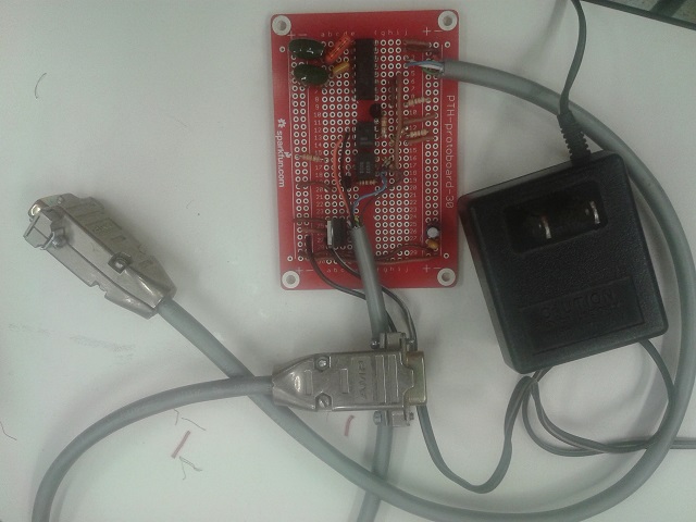
A previous team, which worked on a different PDP-8/L, had developed a RS-232 to current loop circuit that could interface the PDP-8/L with a modern computer via a COM port. The software, “Hyper Terminal”, was available on the professor’s laptop. The settings are reproduced below:
- COM1
- 110 bits per second (baud)
- 8 data bits
- No parity
- 2 stop bits
- Flow control: None
- Emulate: TTY
- Force incoming data into 7 bit ASCII
“Print Test” and “Echo Test” toggle-in programs executed successfully with the laptop’s “Hyper Terminal”.
An online archive of PDP-8/L programs are available on the website “http://bitsavers.org/”. Programs labeled with “PM” are to be loaded with the RIM loader, while programs labeled with “PB” are to be loaded with the BIN loader. After some trial and error, it was found that in order to load the programs through the “Hyper Terminal”, “Transfer -> Send Text File” should be chosen, even though the programs not stored as text files.
Original paper tapes of the BIN loader have been found and compared with the copies. Discrepancies have been found, which implied that the BIN loader used in the previous week may not be correct. Difficulties had been encountered with the paper tape punch while attempting to create copies of the original BIN loader paper tape. Unfortunately, the paper tape jammed and was torn during the copying process. Fortunately, a digital copy of the BIN loader is available on the Bitsavers website. Repairs were made to the original BIN loader paper tape, and multiple good copies were made as backups.
It was found that the “Memory Checkerboard (Low)” and “Memory Checkerboard (High)” were RIM-coded programs, and thus last week’s loading procedure via BIN loader was incorrect. Digital copies of the programs loaded and executed via RIM loader. “Memory Checkerboard (Low)” repeatedly halts at the first memory address it is designed to check (0151) and does not advance to the other memory locations. “Memory Checkerboard (High)” executes as expected and does not halt even after 10 minutes of continuous execution, implying full functionality of every memory location. There is a possibility that “Memory Checkerboard (Low)” failed due to an instruction failure, rather than a memory failure.
The digital BIN loader can be loaded from the laptop, but it subsequently failed to load other digital BIN-encoded programs. The paper tape copies of the BIN loader were successfully loaded, and used to load “Random ISZ Test” from an original paper tape. The test strangely halts immediately on the first pass with an error print to the teletype. Depressing CONT only loops back to the first pass instead of advancing into the second pass as the documentation specifies. If executed with “Halt on Error” and “Suppress Print Info” options, the test runs fully with no errors. It is also possible that a different faulty instruction is causing the error in the default behavior of “Random ISZ Test”.


K’Nex plastic piece as replacement separator for “Line Feed”.
RS-232 Current Loopback Circuit. Interface betweem modern computer COM port and PDP-8/L. Appendix D of “PDP8 Report” for schematics.
Week 7
A summary of the restoration efforts from Week 1 to Week 6 was created for a PowerPoint presentation, as well as an abstract. The file is included below with the filename “PDP-8L Restoration” and “PDP-8L Restoration Abstract” respectively.
A lightly damaged original paper tape of FOCAL (FOrmula CALculator) was repaired by scotch tape and loaded. FOCAL is an interpreted programming language with a complete programming environment (similar to MATLAB). When executed, no initial dialogue was seen, contrary to documentation (DEC-08-AJAB-D FOCAL Programming Manual Jan70). Commands can be inputted, but FOCAL does not recognize any of them and only outputs an “Illegal Command” error message.
An attempt to load a digital copy of FOCAL from the laptop resulted in FOCAL being executed instead of the BIN loader. The problem was due to the START key not registering properly when depressed, most probably due to oxidized contacts. Repeated depression of the START key resolved the issue. The STOP key had a similar issue, and was resolved in the same manner.
Documentation of the BIN loader was found, which explained the BIN loader will halt with non-zero Accumulator if a checksum error occurred. These checksum errors were repeatedly encountered when loading the digital copy of FOCAL from the laptop.
After reloading the original FOCAL paper tape a second time, another checksum error occurred. FOCAL prints the “CONGRATULATIONS!” part of its initial dialogue, but would still respond with an “Illegal Command” error message despite being given valid commands. A third reloading also met with a checksum error, with similar results during the execution of FOCAL. Unfortunately, the original paper tape was torn while making a copy. Repairs were made by manipulating the backspace feature of the paper tape punch to recreate the torn section, which was then affixed onto the original tape as a stabilizer.
During the next copy attempt of the FOCAL paper tape, the teletype produced a jarring noise and stopped working. The gears of the teletype had jammed and a spring had come loose. Suspecting the K’Nex piece which was inserted to fix the “Line Feed”, it was removed. However, that was not the cause of the problem. Further observations revealed that a hook mechanism had come out of sync with the gear it is attached to, causing it to hook and lock onto the gear, thus jamming the whole mechanism. There is another built-in mechanism which prevents the gear shaft from turning in the opposite direction. Manually turning the gear shaft in the opposite direction until it locks, and then turning it in the correct direction, re-syncs the hook. However, the problem reemerges if the teletype is left to idle while powered-on.
Week 8
After unjamming, the teletype produces a squeaking noise which gets progressively louder before the teletype jams again. The squeaking noise sounds similar to that of a lab colleague’s other project, which was caused by friction between the gears of the lab colleague’s K’Nex motors. This inspired further observation of the teletype gear shaft. It was found that the inner gear shaft is made to rotate independently of the outer gears, while the outer gears should rotate only once per key press. However, the outer gears would slip in the direction of the inner gear shaft’s rotation as the squeaking noise gets louder, most probably caused by unwanted friction between the inner gear shaft and outer gears. Once the outer gears slip beyond their intended orientation, the lock mechanism gets erroneously engaged, causing the inner gear shaft and consequently the teletype to jam. Applying silicone lubrication between the inner gear shaft and outer gears alleviated the issue. However, a squeaking noise is still present, albeit at lower a volume, signifying that areas with unwanted friction still remain between the inner gear shaft and outer gears. Periodic application of silicone lubrication is a temporary solution.
Four paper tape copies of FOCAL were made. One of them have been checked with no apparent mistakes, but it consistently loads with a checksum error. If executed despite the checksum error, FOCAL still accepts input but will only output the “Illegal Command” error message. It enters an infinite loop which erases the RIM loader and BIN loader if the CTRL+C “Restart” command is inputted on the teletype. When double-checked against the original paper tape, the copy had no errors.
Another duplicate RS-232 Current Loopback circuit was made. Instead of using a breadboard, the connections and parts are soldered into place for extra stability and reliability.
Programs and Documentation
Increment-AC.txt
PDP-8-Computer-and-ASR-33-Teletype-Programming-Info.pdf
PDP-8L-to-Teletype-Wire-Connections.pdf
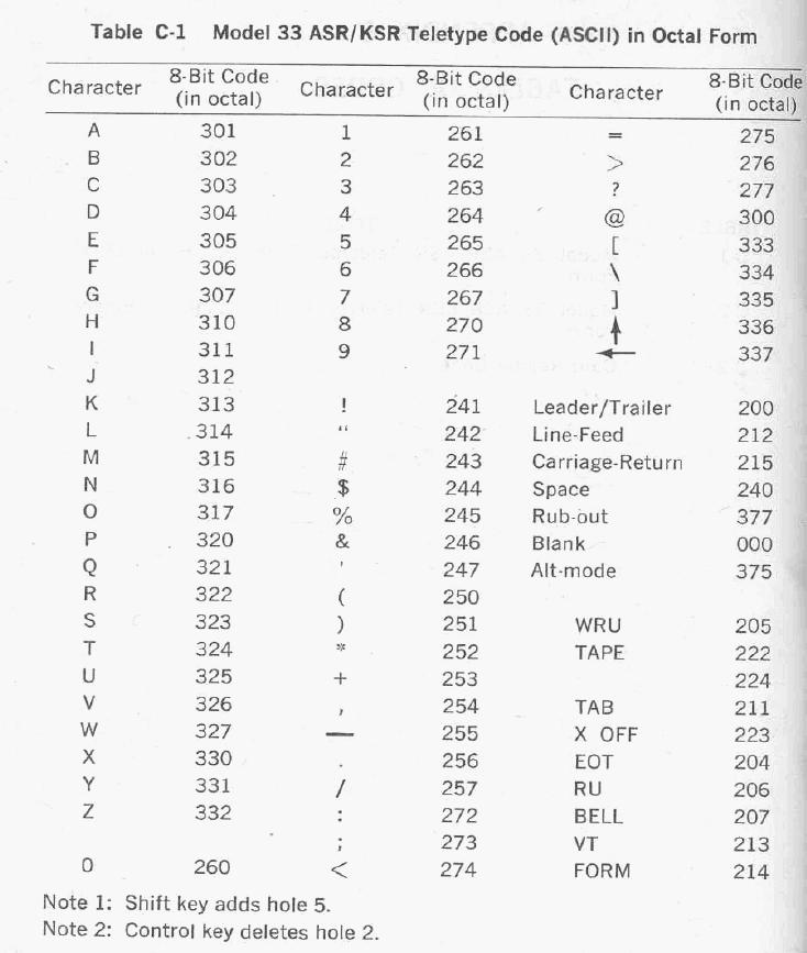
ASCII-Code-in-Octal.jpg
Memory-Check.txt
PDP-8L-Restoration.pptx
PDP-8L-Restoration-Abstract.pdf
Print Test. Accumulator is incremented and used as ASCII code for Teletype.
Loading paper tape program “FOCAL” by teletype Low-Speed Tape Reader.
References
W. Minshew, E. Schwarzenbach, PDP-8/L Minicomputer Restoration and Programming, 2 May 2013.
M. Thompson, W. Stearns, Rhode Island Computer Museum, Website Accessed on: 2011, Correspondence: June 2014.
toggle_in_programs.pdf
» RICM PDP-8/L Restoration Blog
Bitsavers, http://bitsavers.trailing-edge.com/ , Accessed on: June 2014.
DEC-PDP-8L-Users-Handbook-1968.pdf
DEC-PDP-8L-Schematics.pdf
DEC-PDP-8L-Maintenance-Manual-Volume-1.pdf
DEC-08-AJAB-D_FOCAL_Programming_Manual_Jan70.pdf
DEC-08-LBAA-D-BIN-Loader.pdf
» ASR-33 Teletype Manuals
» PDP-8/L Manuals
» PDP-8/L Diagnostic Program Documentation
» PDP-8/L Diagnostic Programs
V. Slyngstad, PDP-8 Stuff, http://so-much-stuff.com/pdp8/index.php , Accessed on: June 2014.